
Project
SMART Photonics accelerates reliable PIC innovation with advanced electro optical characterization
Summary
Organisation: SMART Photonics
Challenge: Ensuring accuracy and long term reliability
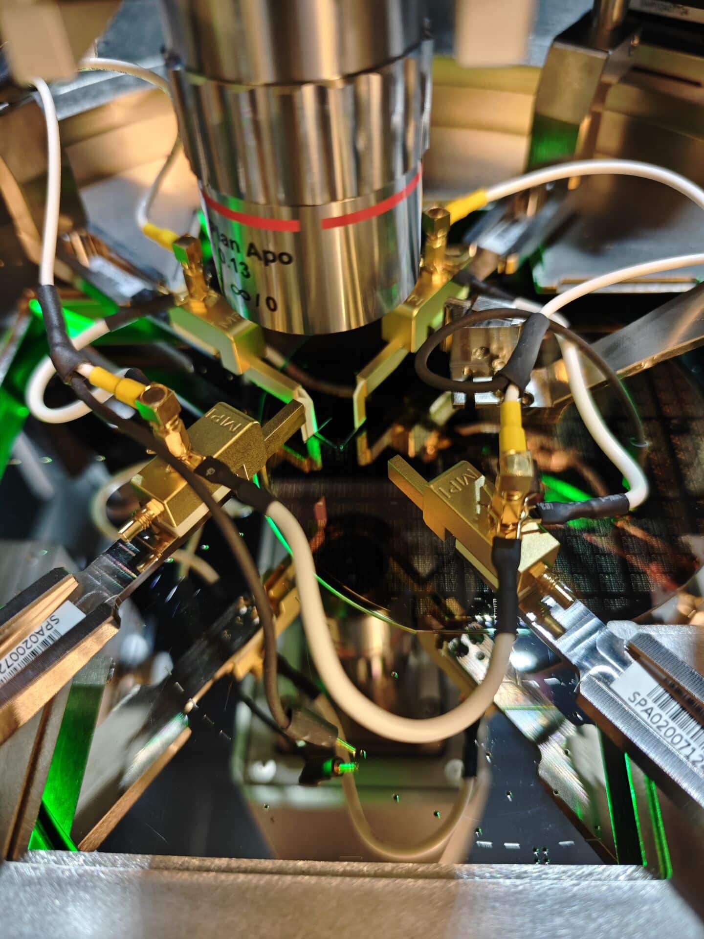
Solution: CN Rood delivered a fully integrated electro optical characterization environment centered around the MPI TS2000 IFE Automated Probe Station. The system is equipped with Silicon Photonics options and PI nanocube fiber positioners for dynamic edge coupling and active alignment. Optical measurements are performed using the Thorlabs PM103 power meter and the EXFO OSA20, while electrical excitation and monitoring are handled by the Keithley 4200A-SCS Parameter Analyzer.
As an independent foundry for integrated photonic integrated circuits (PICs), SMART Photonics delivers scalable solutions for fast growing markets in data and telecommunications, with a strong focus on AI driven computing and high speed communication. By harnessing the power of light, integrated photonics enables a new generation of microchips that are faster, more energy efficient, and more precise. As an independent foundry for integrated photonic integrated circuits (PICs), SMART Photonics delivers scalable solutions for a broad range of fast-growing markets, primarily serving the data and telecommunications industry, with a strong focus on AI-driven computing and high-speed communication. With an operational high volume indium phosphide fabrication facility and a production capacity of up to 5,000 four inch wafers, SMART Photonics is already serving customers across rapidly expanding markets.
The challenge
Ensuring accuracy and long term reliability
The challenge for SMART Photonics lies in guaranteeing performance and long term reliability of increasingly complex photonic devices, both during development and in preparation for mass production. Test and measurement play a crucial role in this process. Serge Evseev, Technical Lead Reliability Engineer, explains: “The test and measurement equipment is of high importance to SMART Photonics, since it enables us to perform high quality electro-optical measurements for our customers.” Accurate electro optical characterization, accelerated lifetime testing, and rapid failure analysis are essential to optimize designs, identify degradation pathways at an early stage, and meet customer and industry reliability standards.
The solution
A fully integrated electro optical characterization environment
To support these goals, CN Rood delivered a fully integrated electro optical characterization environment centered around the MPI TS2000 IFE Automated Probe Station. The system is equipped with Silicon Photonics options and PI nanocube fiber positioners for dynamic edge coupling and active alignment. Optical measurements are performed using the Thorlabs PM103 power meter and the EXFO OSA20, while electrical excitation and monitoring are handled by the Keithley 4200A-SCS Parameter Analyzer. Serge highlights the impact: “The result is that we are able to measure device performance with high accuracy and also study device failure quickly in order optimize designs in a fast way.” The fully automated setup, integrated via TCP/IP and USB and supported by in house developed Python software, enables stable DC characterization and pulsed IV testing under varying thermal conditions.
The result
Stable measurements and scalable production readiness
The results clearly demonstrate the added value of active fiber alignment and precise electro optical control, especially during thermally stressed and long duration tests. As shown in Figure 1, optical power output was measured at +60 °C, +25 °C, and +5 °C, both with and without dynamic fiber alignment. The left part of the curve illustrates measurement performance with active alignment, while the right part shows the situation without active control. Electrical parameters were continuously monitored using the Keithley 4200A SCS. The comparison confirms the importance of active alignment in ensuring measurement stability. The close cooperation with CN Rood played a key role in achieving these results. CN Rood delivered all required equipment and technical support, enabling a highly capable and scalable measurement environment for photonics reliability production and research. With this robust foundation in place, SMART Photonics is well positioned to further increase industrial maturity and move confidently toward the next phase of industrial upscaling.
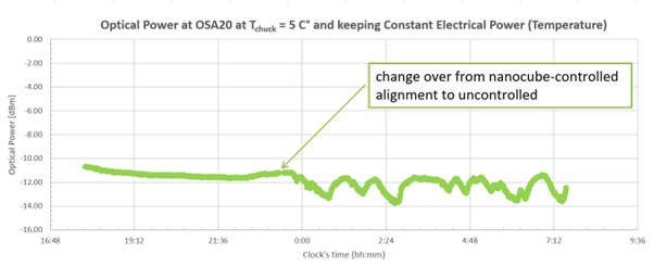
Figure 1: Optical Power Output measured with active alignment (left part of the curve) and without active alignment (right part of the curve). A change from nanocube controlled alignment to uncontrolled state is clearly seen. Electrical parameters are monitored with the Keithley K4200 Parameter Analyzer.
Want to know more?
Ask one of our experts

Bert Broekhuizen
Account Manager & Application Engineer
Semiconductor

Dirk Faber
Technical Application Engineer
Semiconductor, thermal imaging, RF & mmwave applications

Contact
